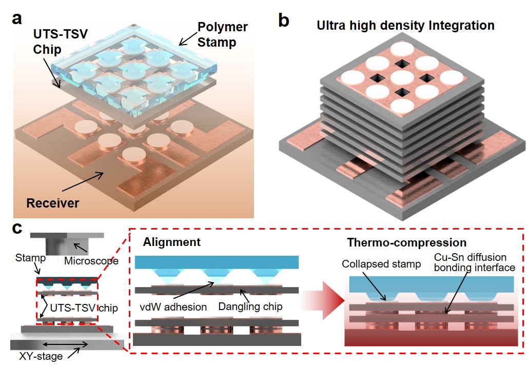
These illustrations demonstrate the stable stacking method of uber-thin semiconductor chips developed by a joint research team of Pohang University of Science and Technology (POSTECH) and the Korea Institute of Industrial Technology. (POSTECH)
By Charles Audouin
A joint research team has developed a stable stacking method of over 10 layers of ultra-thin semiconductor chips, each a fifth the thickness of a human hair, that raises integration density to four times that of high-bandwidth memory (HBM).
Researchers from Pohang University of Science and Technology (POSTECH) and the Korea Institute of Industrial Technology on June 30 said they developed a process of transferring semiconductor chips and simultaneously creating metallic interconnections, resulting in integration density 400% higher than conventional high-performance memory.
As smartphones get thinner, semiconductors need to process enormous amounts of data at extremely high speeds. Thus the semiconductor sector is focusing on vertically instead of horizontally stacking chips.
HBM, which determines the performance of artificial intelligence semiconductors, is built by stacking multiple memory chips layer on layer, thus the technology to stack a high number of chips is considered a key competitive advantage.
The problem is that a thinner chip is more susceptible to bending, warping and fracture, making it difficult to handle during manufacturing.
To overcome this limitation, the team combined two technologies into a single process platform: transfer printing to precisely place chips in their intended positions and In-situ bonding to form metallic bonds simultaneously during chip transfer. This integrates chip transfer, placement and electrical interconnection into a single manufacturing step.
Using the process, the team stably stacked over 10 ultra-thin silicon chips, each about 14 micrometers thick, at low temperatures below 180 degrees Celsius and low pressure below 20 kilopascals.
POSTECH said the stacked chips maintained high alignment accuracy with minimal warping, allowing the stacking of more chips within the same package height.
"This technology is applicable not only to AI semiconductors but also chiplet-based technology, which integrates multiple functional chips into a single package, and micro-LED displays," POSTECH said. "This is expected to emerge as a core foundational technology for developing high-performance AI semiconductors and next-generation memory systems."
The study was published in the online edition of the international academic journal Results in Engineering.
caudouin@korea.kr